![]()
- Products
-
Precision Testing Equipment
LED Chip
Semiconductor components
Bonding Wires
Welding consumables
Solder Materials
Metal Ceramic Substrates
Sinter Materials
Adhesives
Thick Film Materials
Material Systems
-
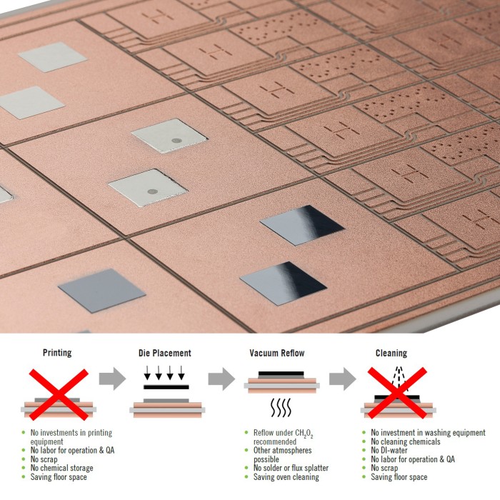
Pre-applied systems simplify processes, decrease investments, improve production yield and reduce production risks. The new Heraeus pre-applied solder Condura(R)+ customized material system fulfills those targets while saving time and money during the die attachment manufacturing process.
In the electronics market the simplification of processes is crucial for higher yield with lower costs and minimized risks. In order to support these key targets, Heraeus offers pre-soldered Condura(R)+ alumina substrates for die attachment.
This new material system combines Heraeus’ premium metal ceramic substrate with flux-free solder pads that have already been pre-applied. This simplifies the die soldering process dramatically since solder paste printing and flux residue cleaning are not required. Furthermore, since the solder material is just a metallic alloy and does not contain any solvent, solder splattering is avoided.
The special solder pads are positioned precisely at the correct location and are available in variable forms and volumes matching to the module design. Fixation dots deposited on the solder pads ensure that the dies do not move after placement. Upon reflow, the fixation material vaporizes without leaving any residue.
Advantages at a glance:
Faster, more efficient, cost saving production process:
50 % fewer process steps for die soldering, since solder printing and cleaning step are not required
Lower investment in equipment and cleaning materials, resulting in production cost savings
Improved yield, through less rejected goods due to splatter and damage during the cleaning process
Less reflow oven maintenance costs due to less contaminations with solder residues
Your benefits in working with Heraeus:
Exactly the right solution for your application, adapted to your needs
Quicker time to market due to unique expertise of matching materials to systems with maximum performance and reliability
High innovation capabilities
With our in-house application center we are able to:
Perform the complete module back-end assembly
Build prototypes of electronic modules
Run tests at module level as our customers do
Go to see more:https://www.heraeus.cn/cn/
Power electronics in industrial use:
Our Condura(R)+ substrates are recommended for power electronic modules (e.g. current inverters) using MOSFETs or IGBT semiconductor elements and diodes for widespread application fields in the industrial sector: electric motor drives, e.g. in tooling machines, cranes, textile-processing equipment, automation equipment, etc.
Pumps
Welding machines
Electrical industrial vehicles (e.g. power drives for forklifts)
Induction heating
Industrial drives (e.g. escalators, conveyor belts, elevators, robots, and servo drives)
Uninterruptable power supply to. data centers, hospitals, etc.
Drillings for natural resources (e.g. oil and gas)
Energy technology (e.g. photovoltaics, wind turbines, and energy distribution)
White goods (e.g. air conditioners, washing machines, refrigerators, and warm water pumps)
Automotive and traction:
As high-performance circuit carriers for power electronic applications:
In such groups as power steering, start-stop systems, air conditioning compressors, water pumps, oil pumps, brakes, etc.
Converters for hybrid or electrical power train
Battery chargers
Inductive charging systems
DC-DC converters
Rail vehicles such as locomotives, subway trains, trams and cable cars, etc.
Communications:
Uninterruptable power supply (UPS) to telecommunication centers (e.g. RF amplification systems)
Further markets:
There are many examples of further markets in which DCBs are already being applied, such as medical technology (MRT, CRT), aerospace, radar systems, heavy building machinery, and looking towards the future, increasingly in agricultural vehicles and aircraft.
Go to see more:https://www.heraeus.cn/cn/
Alumina Condura(R)+ substrate
Alumina ceramic Al2O3 (96%)
Thicknesses: 0.25mm/0.32mm/0.38mm/0.63mm
Direct Copper Bonding Cu-OFE
Thicknesses: 0.2 mm/0.25 mm/0.3 mm/0.4 mm
Single Unit or Master Card size 7-" x 5-" (usable area)
Surface finish: bare Cu (others to be agreed)
No visible splatter
Find more technical details here .
Solder pads
Alloy: SnAg3.5, SAC 305, other alloys to be agreed
Size: based on customer requirements
Thickness: based on customer requirements, typically ≤ 60 μm after die attach
Various solder material thicknesses and areas can be placed on the substrate
Fixation dot
Vaporizes without leaving any residue (checked with Auger spectroscopy and bonding wire pull & shear tests)
Die
Metallization: Solderable functional surface: e.g. Ag or Au
Size: based on customer requirement
Die soldering
Process: Reflow in active atmosphere (e.g. formic acid CH2O2). We can support you to design your process conditions such as reflow oven
profiling.
Total void rate: ≤ 5 % of the wetted area
Max. void size: ≤ 0.5 % of wetted area
Splatter: no splatter visible
Residue cleaning: not required
Go to see more:https://www.heraeus.cn/cn/